https://doi.org/10.1140/epjb/s10051-025-00987-2
Regular Article - Solid State and Materials
Study on the electronic structure and optical properties of InSb/WSSe van der Waals heterostructure
School of Physics and Electronics Information, Yunnan Key Laboratory of Opto-Electronic Information Technology, Key Laboratory of Advanced Technique and Preparation for Renewable Energy Materials-Ministry of Education, Yunnan Normal University, 650500, Kunming, People’s Republic of China
a
lvxiankui@163.com
b
220001@ynnu.edu.cn
Received:
12
April
2025
Accepted:
11
June
2025
Published online:
21
June
2025
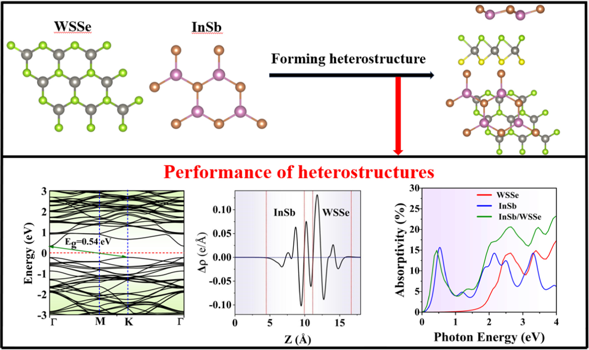
Van der Waals heterostructures offer promising avenues for designing optoelectronic materials with tailored functionalities. Here, we employ first-principles calculations to investigate the structure, electronic, and optical properties of a novel InSb/WSSe heterojunction. The optimized structure reveals a stable interlayer spacing of 3.229 Å and exhibits type-II band alignment with a direct bandgap of 0.54 eV. Charge density analyses indicate electron transfer from the InSb layer to WSSe, resulting in an intrinsic interfacial electric field directed from InSb to WSSe. The heterojunction features a work function of 5.12 eV and demonstrates a notable enhancement of 37%. The InSb/WSSe heterojunction effectively combines the optical advantages of its constituent materials. Optical absorption is significantly boosted across the infrared, visible, and near-ultraviolet regions, with peak absorption in the visible spectrum reaching 20.63%—representing 44% increase than the monolayer components. In the infrared region, the absorption rate of the heterojunction breaks through from 0 to 14.96%. In the near-ultraviolet region, absorption improves by 26.6% compared to monolayer WSSe. Moreover, compared to monolayer WSSe, the heterostructure effectively suppresses optical transmittance (84.36%) and exhibits distinctive reflectance peaks. These findings highlight the InSb/WSSe heterojunction as a promising platform for broadband light-harvesting and next-generation optoelectronic applications.
Copyright comment Springer Nature or its licensor (e.g. a society or other partner) holds exclusive rights to this article under a publishing agreement with the author(s) or other rightsholder(s); author self-archiving of the accepted manuscript version of this article is solely governed by the terms of such publishing agreement and applicable law.
© The Author(s), under exclusive licence to EDP Sciences, SIF and Springer-Verlag GmbH Germany, part of Springer Nature 2025
Springer Nature or its licensor (e.g. a society or other partner) holds exclusive rights to this article under a publishing agreement with the author(s) or other rightsholder(s); author self-archiving of the accepted manuscript version of this article is solely governed by the terms of such publishing agreement and applicable law.